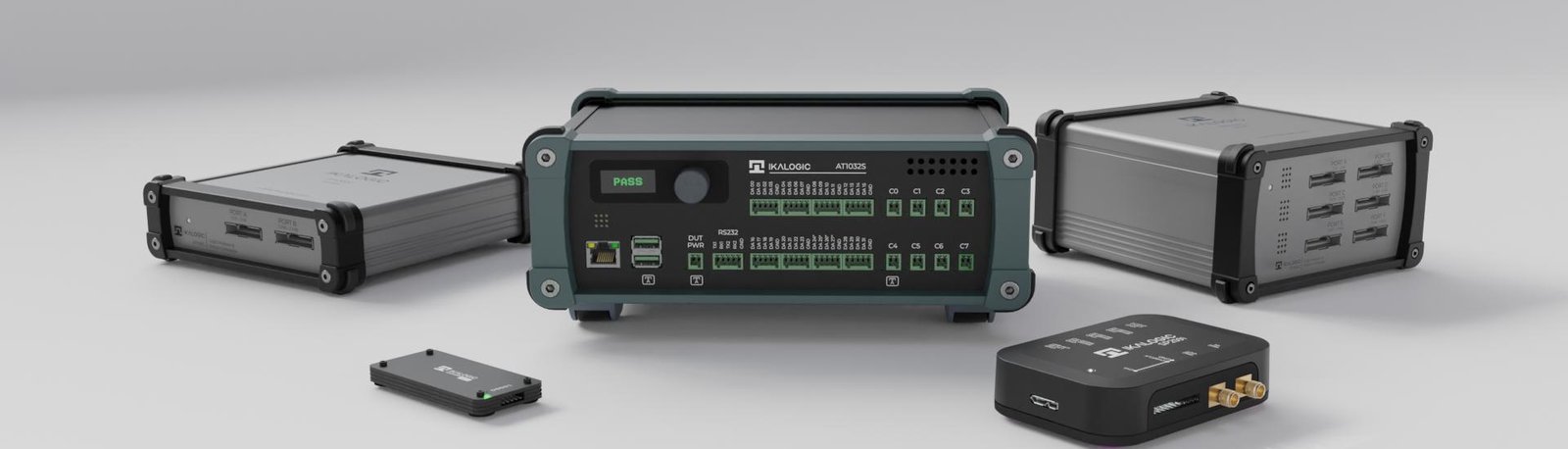
Test & Measurement Instruments
For electronics engineers
From compact logic analyzers to advanced test sequencers, Ikalogic builds high-performance instruments trusted by electronics engineers worldwide.
- Logic Analyzers
- Pattern Generators
- Test Sequencers
- RF Switches
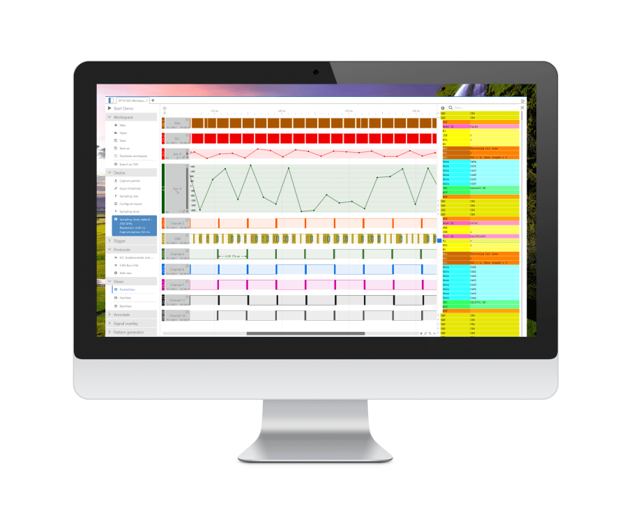
Professional Logic Analyzers for Embedded Engineers.
Capture and decode I²C, SPI, 1-Wire, CAN bus, UART, and more. Set precise triggers, sync with other instruments, and never miss a bit.


Pattern Generators with Built-in Logic Analysis.
Generate and capture digital signals with a single instrument — ideal for semiconductor testing, QA and DFT (Design For Test) workflows.
Automated Functional Testing for PCBs and Products
Streamline PCBA validation using a modern approach to test sequencing. Interface with bed-of-nails or standard connectors, and customize every step with a powerful, scriptable API .


Diverse RF Switching, Made Simple
Meet the CS8000 Series – our 8 GHz switches designed for demanding lab and production environments. With ultra-low insertion loss, USB control, and SMA trigger input for synchronized switching, it’s the perfect tool for RF testing, routing, and automation.
They trust us
Ikalogic is a trusted partner for leading companies and institutions in the electronics industry.


Inquire about our solutions
Not sure which product fits your needs? Want to explore a custom project? Let’s start the conversation.