The Memory View: Read Your Target's Memory Straight From a Capture

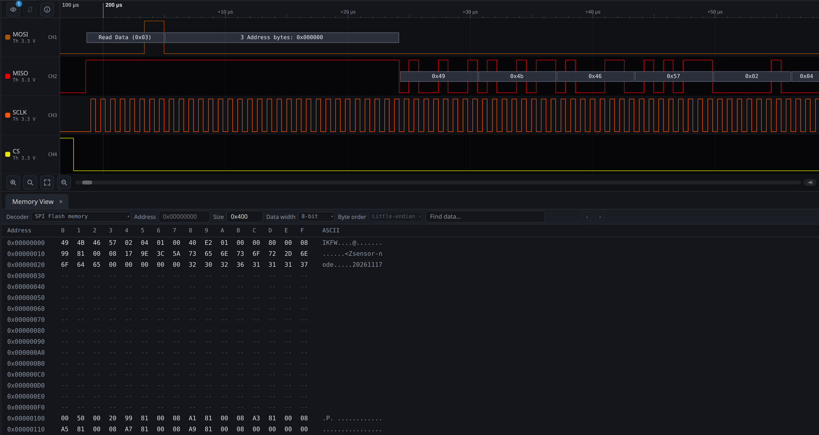
When a microcontroller boots from an SPI flash, the capture holds everything it read: the image header, the vector table, the settings. The decoder lists those bytes in time order, frame by frame. What you usually want to know is what sits at address 0x100.
The Memory View answers that. A decoder places each byte it decodes at the address it was read from or written to on the target, and ScanaStudio shows the result as a memory dump, with the target's addresses down the side.
Download ScanaStudio V6From Bus Frames to Addresses
The Hex View and the Packet View follow the capture: one byte after the other, each tied to the samples it came from. The Memory View follows the target. The decoder knows the address of every byte, because the address is on the bus: the three address bytes after an SPI flash Read Data command, or the TAR register of an SWD debug port. It hands each byte to the view with that address.
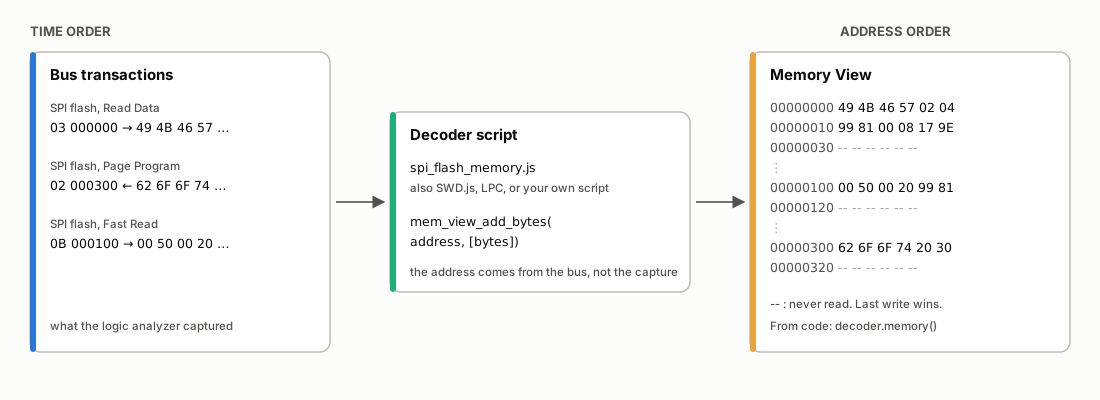
Transactions arrive in time order. The Memory View sorts their bytes by address.
Two rules make the view easy to read. An address the bus never touched shows as --, which is different from a byte read as 00 or FF. And when the same address is read or written several times, the view shows the last value.
Three decoders fill the Memory View today: SPI Flash memory, SWD and LPC. Each one has a new option that selects what goes in the view.
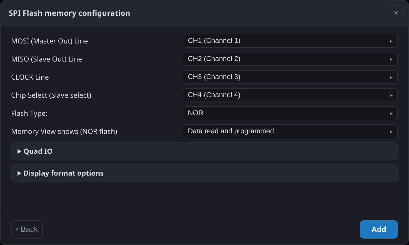
The SPI Flash memory decoder shows the data read and programmed, or only one of the two.
SPI Flash: What the Bootloader Read
The captures in this post come from the demo signals of each decoder, so you can reproduce them in ScanaStudio without any hardware. The SPI flash demo plays a microcontroller booting from a Winbond W25Q128. On every boot it reads the image header at 0x000000, the vector table at 0x100 and a settings block at 0x200, then writes one line to a boot log at 0x300.
The image at the top of this post is the first read of the header. The Memory View shows the 48 bytes at their addresses: the "IKFW" magic, the version, the image name and the build date are readable in the ASCII column.
At 0x100, the vector table is easier to read as 32-bit words. The Data width setting groups the bytes by 1, 2 or 4.
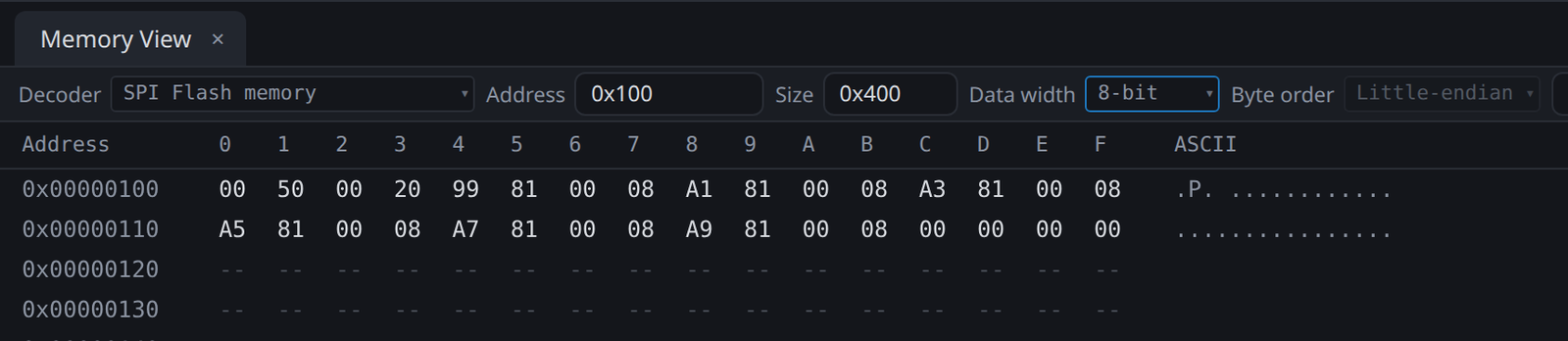
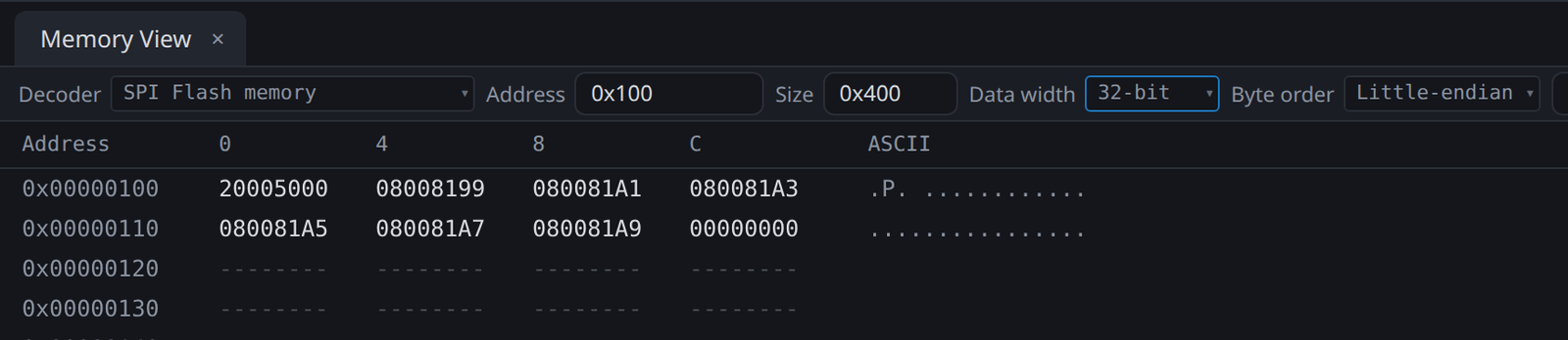
The same 32 bytes as bytes and as 32-bit words: the initial stack pointer 0x20005000, then the reset handler at 0x08008199.
The Byte order setting decides how the words are built from the bytes. The decoder can suggest one for its target, and you can change it at any time.


The "IKFW" magic reads 0x57464B49 as little-endian and 0x494B4657 as big-endian.
The settings block at 0x200 shows why -- matters. The bootloader reads 48 bytes: the text, then the end of the block, still erased. The erased bytes show as FF because they were read. The rest of the page shows -- because nobody read it.
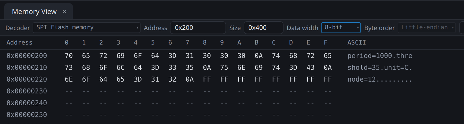
FF: read, and erased. --: never read.
The boot log at 0x300 is written with Page Program commands, one 16-byte line per boot. The writes go in the view too, at the addresses they were programmed to. The log fills its 256-byte page and starts again at the top, which is easy to follow in the view: the lines for boots 48 and 49 sit above the lines for boots 42 to 47.
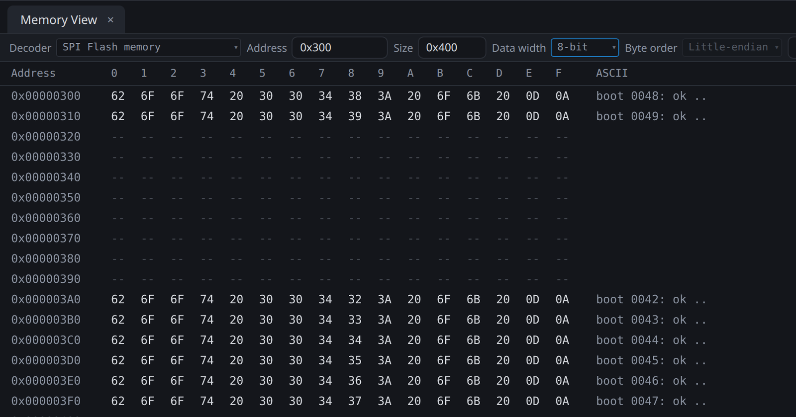
Eight boots in one capture. The log wrapped after boot 47.
SWD: The Debugger's View of RAM
The same idea works for a debug port. When a debugger reads a Cortex-M's memory over SWD, it writes the address to the TAR register of the memory access port, then reads DRW once per word. The SWD decoder follows TAR, the access size and the address increment, and places every word read or written at its address.
SWD has one more detail: an access port read returns the data of the previous read. The first DRW read of a block returns nothing useful, and the last word arrives through RDBUFF. The decoder keeps track of that, so each word lands at the address it was read from.
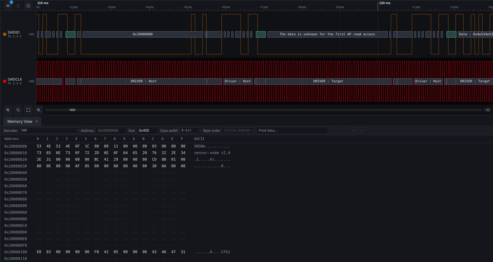
TAR = 0x20000000, then DRW reads. The word 0x4E534E53 arrives with the second read and belongs to address 0x20000000.
In the demo, the debugger reads a 64-byte state block at 0x20000000 and writes a configuration block at 0x20000100. In 8-bit mode, the firmware name and the "CFG1" tag the debugger wrote are readable at once.
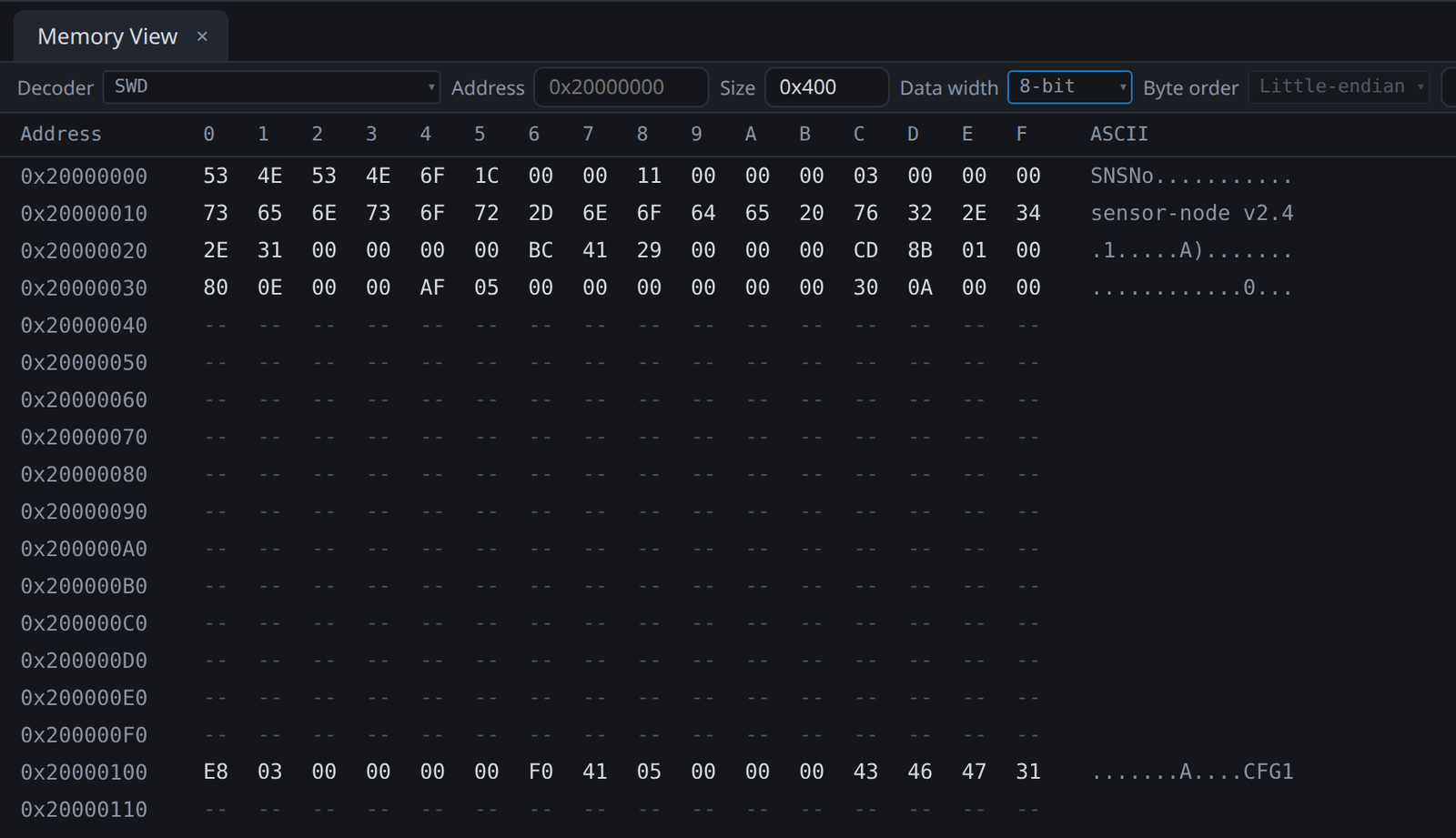
What the debugger read at 0x20000000 and what it wrote at 0x20000100.
LPC: Firmware and Memory Cycles
On a PC motherboard or an embedded x86 board, the BIOS or UEFI firmware is fetched over the LPC bus. The LPC decoder places the data of memory cycles, firmware cycles or I/O cycles in the Memory View, at the address of each cycle.
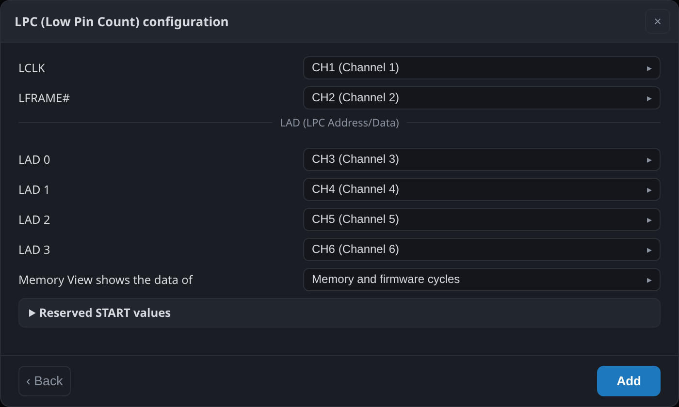
The LPC decoder selects which cycles fill the view.
Copy It Out
A right click in the view opens the copy menu. Copy all copies the window as a dump, with the addresses and the text. Copy data only copies the words alone. Copy raw bytes copies the bytes as one run of hex in address order, whatever the data width and byte order, ready for a hex editor or a diff.
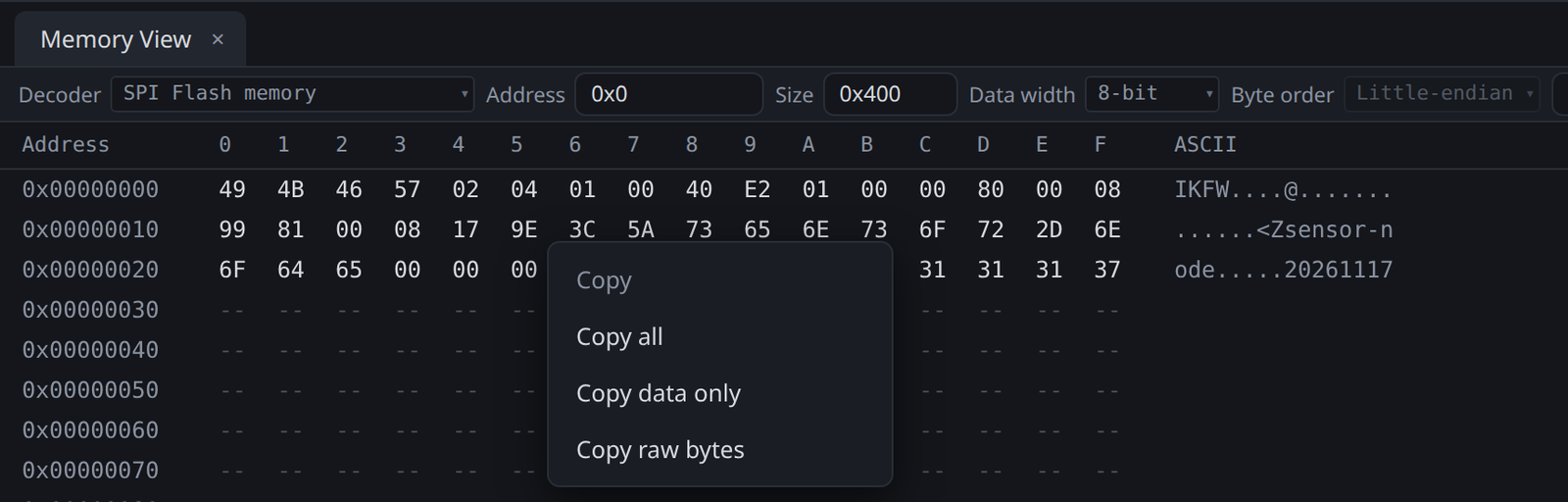
Your Own Decoder
Any decoder script can fill the Memory View with three functions. A decoder for an I²C EEPROM, a parallel memory bus or a proprietary protocol needs one call per block of data it decodes:
function on_decode_signals(resume)
{
  if (!resume)
  {
    ScanaStudio.mem_view_set_base(0x0000);  // where it opens
    ScanaStudio.mem_view_set_endianness("big");
  }
  // ... decode a read: the address, then the data ...
  ScanaStudio.mem_view_add_bytes(address, data_bytes);
}
The address is the target's, from 0 to 0xFFFFFFFF. The base address and the byte order are suggestions: the user can change both in the view. The functions are described in the protocol decoding chapter of the scripting manual.
From Code
The Memory View is also available from the ScanaStudio SDK, in Python, NodeJS, Rust and C. decoder.memory() (instance_memory in Rust and ss_mem_read_instance in C) returns it in pages, each byte with its address. That makes a production test a few lines long: capture the boot, then compare what the bootloader read with the file that was flashed.
from ikalogic_scanastudio import ScanaStudio

with ScanaStudio.connect() as server:
    device = next(d for d in server.devices() if not d.demo)
    ws = server.create(device.key)
    flash = ws.decoders.add("spi_flash_memory.js", {
        "ch_mosi": 0, "ch_miso": 1, "ch_clk": 2, "ch_cs": 3})
    ws.capture.run(samples=5_000_000,
                   sample_rate=250_000_000)
    flash.wait()

    # the whole Memory View, page by page
    # (a later write to an address wins)
    memory, offset = {}, 0
    while True:
        page = flash.memory(offset=offset, count=5000)
        memory.update((b.address, b.value) for b in page.bytes)
        offset += len(page.bytes)
        if not page.bytes or offset >= page.total:
            break
    print(f"{len(memory)} bytes read, "
          f"from 0x{min(memory):06X} to 0x{max(memory):06X}")

    # the header the bootloader read, against the flashed file
    header = bytes(memory[a] for a in range(0x30))
    with open("sensor-node-2.4.1.bin", "rb") as f:
        expected = f.read(0x30)
    ok = header == expected
    print("image header:", "OK" if ok else "MISMATCH")
    ws.close()
256 bytes read, from 0x000000 to 0x0003FF
image header: OK
Conclusion
The Memory View turns a bus capture into a memory dump of the target: what the firmware read from its flash, what a debugger read from RAM, what was written and where. The SPI Flash memory, SWD and LPC decoders fill it today, and any decoder script can fill it with one function call.
It needs ScanaStudio 6.0.23 or later. The updated decoders arrive through the script manager.
Download ScanaStudio V6 - Read the scripting manual - Contact us with your questions